
See more than ever before
AIM Solutions creates advanced 3D imaging technology for semiconductor inspection and metrology.
Hardware measures. Software reveals.
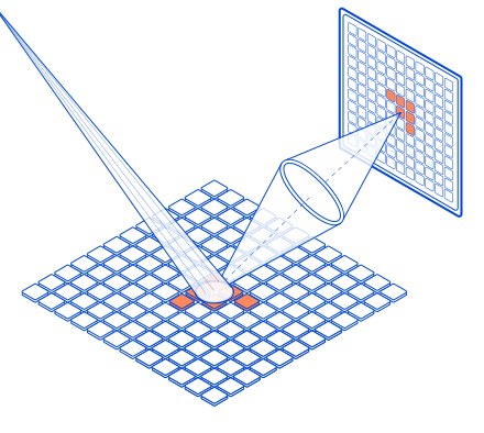
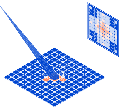
By replacing hardware-heavy & complex optical systems with a hybrid of measurement and computation, we bring high-resolution 3D metrology to back-end applications.
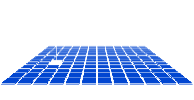
Native 3D
We can produce the interferometry-grade 3D images critical for hybrid bonding and future applications, using a simpler system than complex optics.

Patented inline throughput
Our breakthrough continuous scanning technology is ready for industrial production and produces throughput at >1 wafer per hour.

Wavelength-agnostic
By offering lateral resolution, height accuracy and defect sensitivity we can ensure that all performance specs scale with the wavelength, except for the cost

Easy to scale
The precision that is hard to manufacture, we compute. The precision that is hard to replicate, we own.
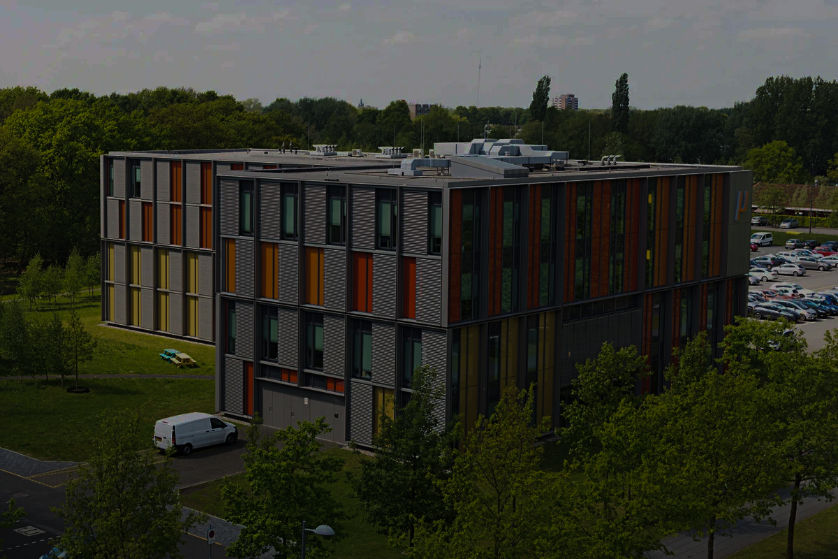
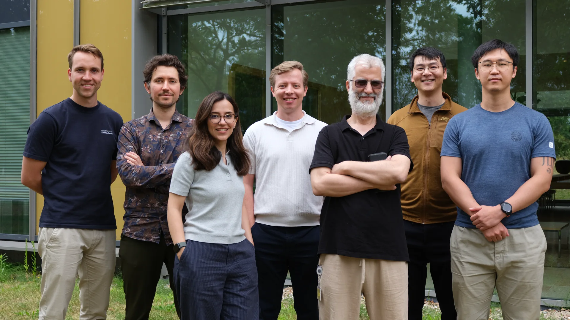
We are an early-stage deep-tech startup based in Eindhoven, in the Netherlands.
Our team of former research scientists and semiconductor professionals is developing an industrial semiconductor inspection and metrology machine using computational imaging.
By offering industrial-level throughput 3D profiling we can make fabrication more cost-effective and accelerate semiconductor innovation across the industry.
Explore Open Positions
We're looking for driven builders, engineers, and scientists to shape the next-gen semiconductor inspection and metrology technology.
Reach out to discuss technology partnerships or pilot programs.
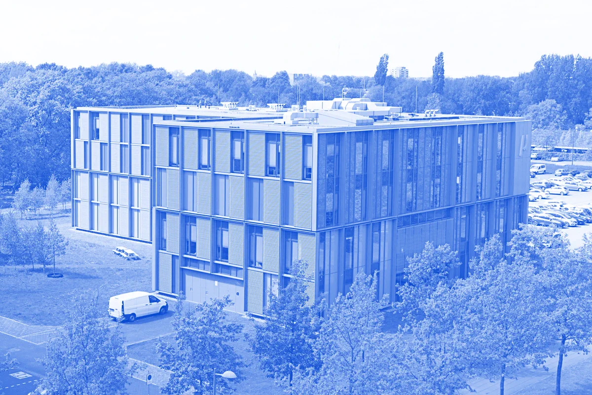
Mu Building
5656 AE Eindhoven
The Netherlands

