
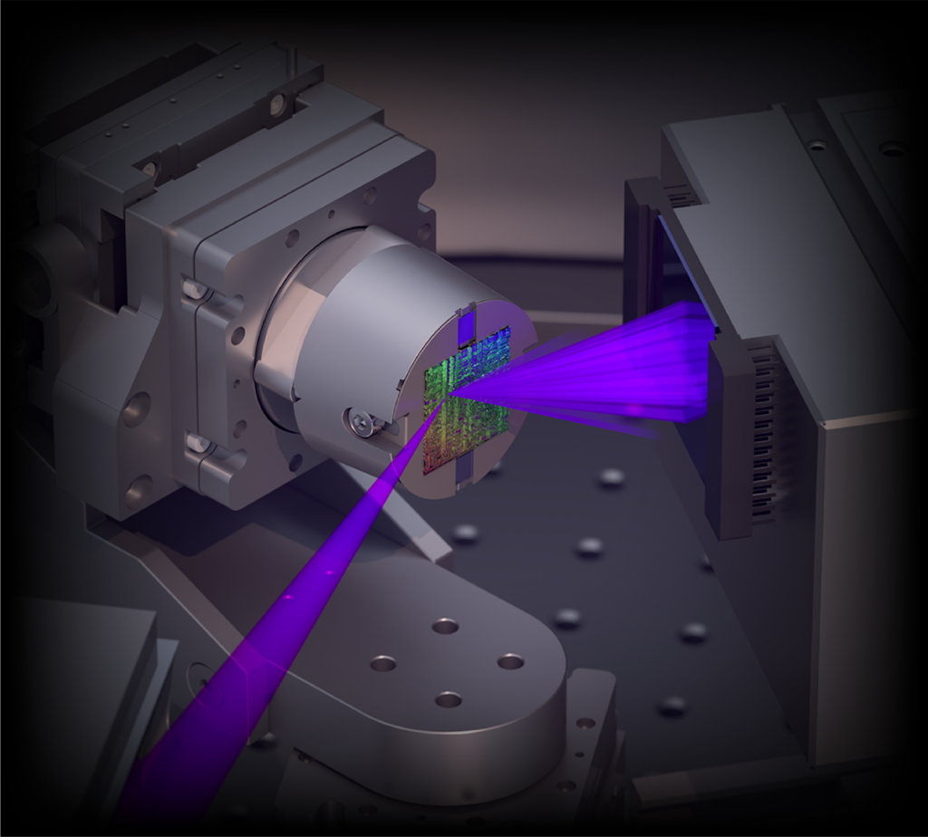
EUV Defect Inspection
We use EUV light to inspect defects in the sample.
Our computational imaging technology significantly reduces equipment costs while providing superior resolution and sensitivity.
Superior Resolution
Using EUV light for imaging provides sufficient resolution to identify defects for the advanced nodes of semiconductor manufacturing.
Superior Sensitivity
Computational imaging enables the identification of defects by providing phase information sensitive to material and structural changes in the EUV band.
Reduced Costs
Replacing the imaging system with our algorithm eliminates the need for complex and expensive EUV optics in the equipment.
Computational Imaging
- Reconstruction of images from diffraction patterns using a powerful algorithm.
- Offering both amplitude and phase information of the sample function.
- Capable of calibrating and correcting system errors using our algorithm.
- AI-ready: Integrating AI (neural networks) into our algorithm improves the performance.